Everything started when i replaced the brushed motor of my mini lathe with a new higher torque (from far East) brushless dc motor. It was for sale as a replacement part for sewing machines but did a great job for the mini lathe. There was no cutting force that could stop this motor.

On a rebuilt that i did on my mini lathe and as i had everything teared down i thought it would be a great idea to add some extra features to my brushless dc controller. Features like the option to stop/lock the motor in a specific position or turn it a specific number of degrees or even get the servo position encoder readout and use it to control a step motor for driving the leadscrew which thereinafter will automatically cut threads without the need of manually gears changing in the gearbox. (This is another ongoing project for automatic thread cutting which included an extra rotary encoder for the spindle positioning). “Kill two birds with one stone”.

So i start looking the controller PCB ( OD-P05-001-54 F2H0794-A0 UIDO or ODIN depending on which orientation you read it ) trying to understand how it operates.

It looked to have an onboard SMPS, some drivers and fets for the H-bridge, some logic gates and schmitt triggers and a central microcontroller to control everything onboard. The mcu has a label of 8132Z008 0C022 with no available information online. At least all my searches didn’t return any useful information. Nearby the mcu there was a pinhead 3×2 and measuring the voltages across the pins it gave a good chance to be an AVR ISP. I thought it would be a good idea to connect the AVR ISP and try to read this MCU and check if there is a known AVR under this package or at least a copy of. Since the voltage and ground pins where aligned there was no chance of short circuiting something that will make the magic smoke. So everything was straight forward.

I connected the AVR ISP between my (charging) laptop and the PCB and…. i plugged the PCB to the mains power.

……

……

Everything went black! I was wondering what did go wrong? I unplugged it from the mains and i walked down to the electrical panel. The Earth-leakage circuit breaker (ELCB) and the circuit breaker of the mains plug interrupted the mains! WoW! It looked to be something serious! I reset the ELCB as well as the circuit breaker and i started looking for the cause. I realised that the laptop was shut down! That was a really bad omen. Fortunately pressing the power on button boot the laptop normally. It seemed to have minor losses and of course lessons learned! Never again an electrical device mains powered connected to my tools without an isolation transformer. This was also the reason i built an isolation box with 1:1 transformer, a fuse box and a seperate ground banana plug to connect it only when needed.

On the PCB nothing seemed to get blown so i tried to power it on with nothing connected on it and yes it did power up but it didn’t function any more. The shock was big enough to blow the mcu.

Still, it wasn’t clear to me what happened. It looked to me for a short circuit from the PCB to the earth’s ground but what was that? And the adventure just began. There was no choice anymore from reverse engineering the controller and understanding how it did work and then try to build a safer and more robust controller implementing all of my extra requirements/features.

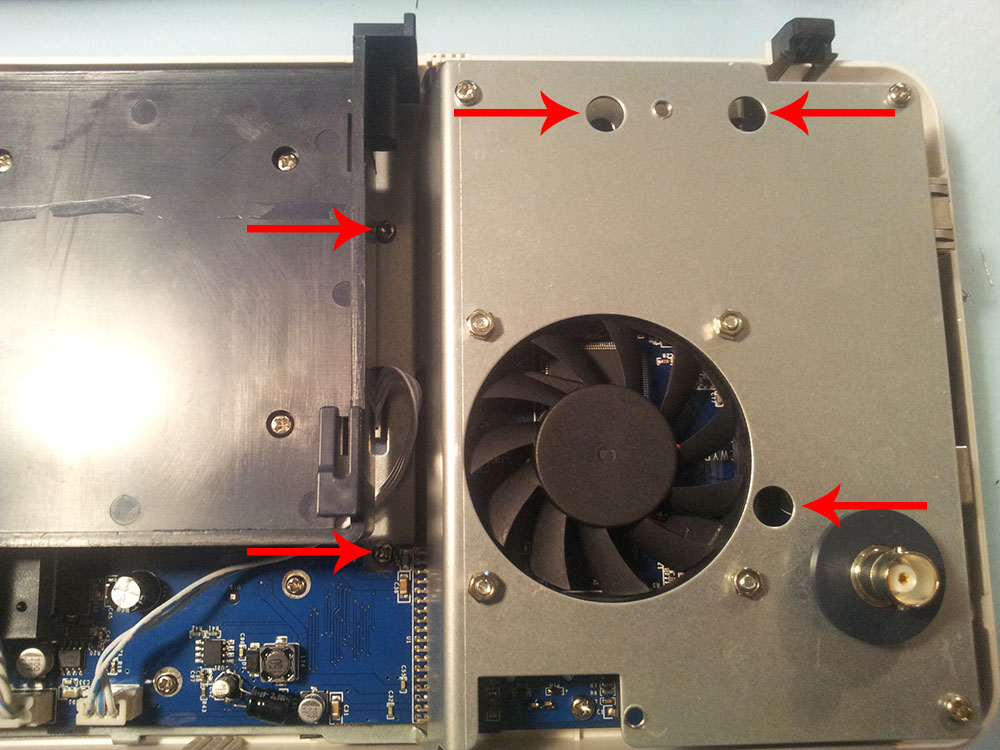
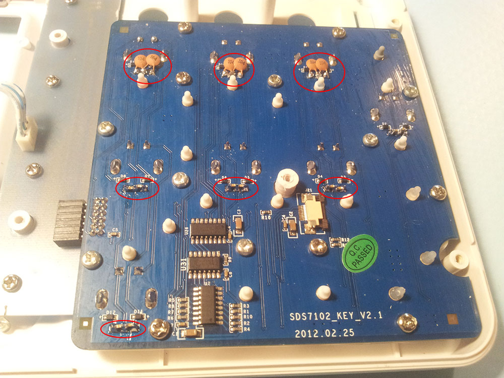
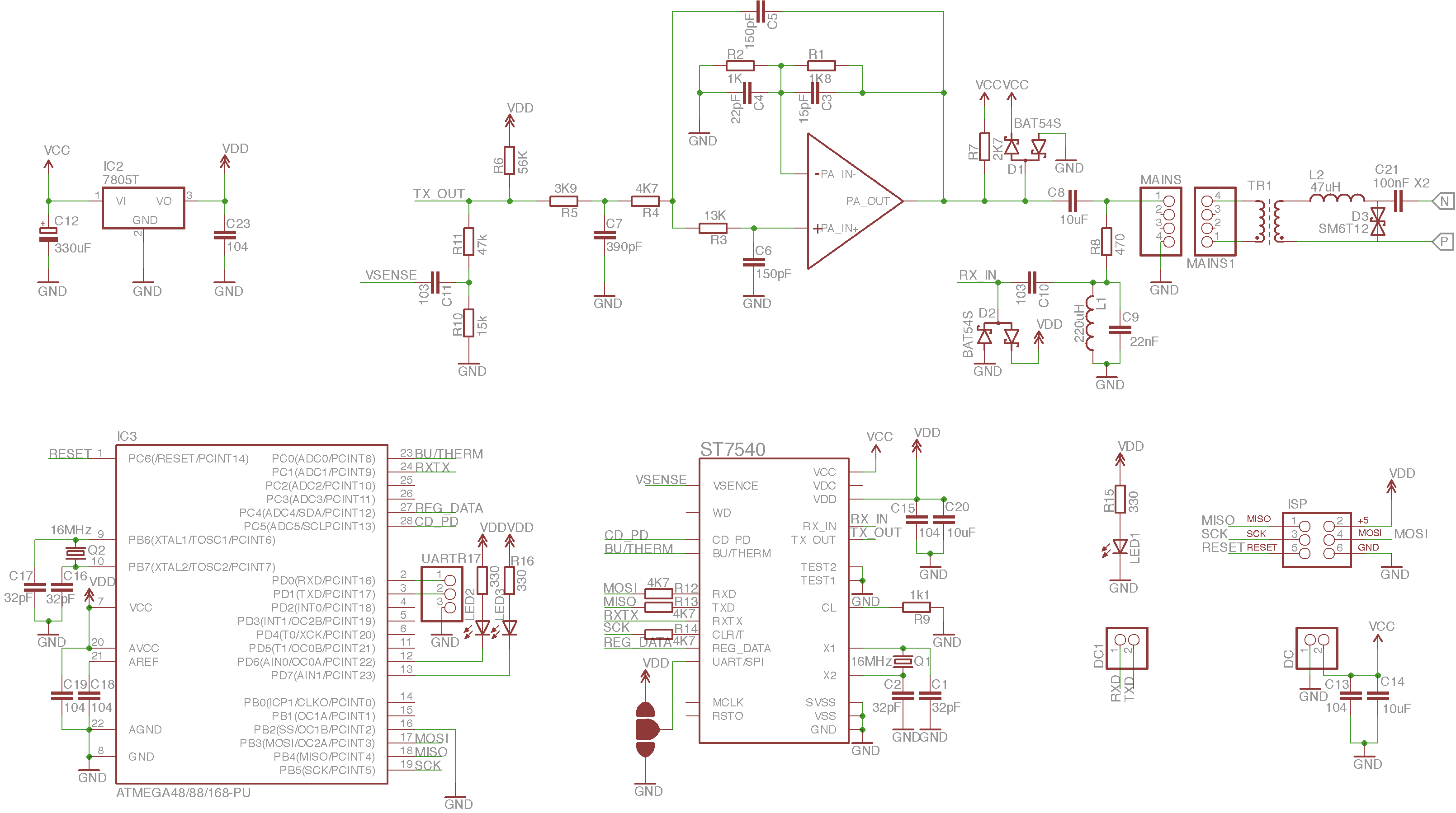
Step by step using my multimeter and supplying the PCB with 5Volt on VCC pins when required i started reverse engineering it. After two weekends of work here you have all the outcome of my spent hours in schematics.

We start with the power supply

The power comes from the mains passed through a huge safety fuse of 10A ! i don’t know what is going to get blown first here. Then there is an X2 capacitor and the Rectifier. Following the rectifier a 500 Ohm 1watt resistor is used to slow charge the two in series electrolyte capacitors of 680uF/250WV during startup. As i can imagine they are used in series to increase the voltage rating. Just a few milliseconds after startup Relay1 arms from the 15Volts produced by the SMPS (not yet discussed) and the RT1 is by passed. This is it. The output is a ~ 330V not isolated DC power. This is the BLDC (brushless DC) motor High Voltage used in the H-bridge. Believe it or not. The – (minus) of the mains full wave rectifier is directly connected to the PCB digital ground! Is something coming to your mind? I don’t know about you but i already make some imaginations… When i connected my AVR ISP onboard actually i did connect the – (minus) of the rectifier to the earths ground through my laptops usb. It doesn’t sound that safe does it? By connecting the minus of the rectifier to the earths ground, means that the mains is shorted to ground on each negative cycle of the AC. About 50 times per second for a 50Hz mains. This is the first design i see with no mains isolation. Attention! The same could have happened if i was trying to probe the circuit with my oscilloscope hooking the scopes ground on the digital circuit GND for reference.

Following the 330V DC we meet the SMPS that i did recognize on my first look but unfortunately i wasn’t so suspicious to take a closer look and see that there was also a second not isolated power. I imagined that everything was powered from the output of the SMPS.

On this smps there are two secondary windings producing 5Volt and almost 15Volt (14.7 measured). The 5Volts are further regulated by the TL431K linear regulator . I think there is no need for any further analysis here.

Close to the SMPS there was an optocoupler with a transistor and a higher wattage resistor that caught my eye.

It looked to be something separate from the SMPS but neither a piece of the digital circuit. After some continuity measurements i found that this was a circuit that grabs the mains frequency and supplies it in TTL Voltage levels to the digital circuit and specifically to the MCU directly.

Could this be a clock for some operations? Or maybe a way to identify if the board is powered by 110V/60Hz or 220V/50Hz mains power and adjust the duty cycle of the H-bridge? I don’t know but make guesswork as the mcu has gone and i can’t take real measurements on the PCB while running.

Turning to the Digital side i started by reversing the side of the Servo Encoder received signal path.

The encoder consisted of 3 pin outputs. The signals once on board are pulled up by resistors and decoupled by capacitors. Then they are passed through a schmitt trigger/inverter (74HC140A) twice to clear and invert twice the signals. The output of the schmitt trigger feeds directly the MCU where the MCU can identify the position of the motor’s rotor. These signals also feed two XOR gates (74HC86). My guess is that these gates are used to create a pulse output corresponding to the motors rpms. Then it could be used a dedicated hardware MCU interrupt just to count the motor rpms and the 3 encoder signals when there is the need to know the position of the rotor. Maybe on the startup sequence?

On the side of the H-bridge circuit there was an IC standing out from the others with some resistors around it.

A closer look showed me that U6 is an LM393 with two Op-Amps inside. My first guess was that this comparator is used to adjust the supplied voltage to the motor but after drawing the circuit on paper i realised that this should be an over current protection. A cheat to this was the R31 R015/3Watt resistor nearby which drove me to the conclusion of the overcurrent protection even before finishing the circuit drawing.

The R31 is used as shunt resistor. One side is connected to Ground and the other side is connected on low sides of the H-bridge so it can sense the current draw of each motor phase. The first op-amp is used to compare and sense the current and the second/followed one is used to convert the output of the first one to the logic level of 0-5V (open collector output). Something like analog to Logic converter. Running this circuit on spice it results that overcurrent protection is active High when current load is more than ~ 2 Amperes across the shunt resistor. The mcu pin on the other side could be there as an analog input to also read the current sense voltage drop but i’m not sure for this.

And now the real thing.

The H-bridge and it’s driving circuit.

Starting from the MCU side, the signals are first pulled up. Then depending if they drive the High side of the H-bridge or the Low side they are feed to a NOR (74HC02D) or OR (74HC32D) accordingly. These gates are used in combination with the overcurrent protection to directly cut off the driving of the H-bridge in an overcurrent detection. HIN, is active high but LIN is active low. Using a NOR gate on High sides when the overcurrent is on the one side of the NOR input is going to be High resulting always an output of logic 0 which means the H-bridge High side to be deactivated. Respectively using an OR gate on the Low sides when the overcurrent is on the one side of the OR gate input is going to be High resulting always an output of logic 1 which deactivates H-bridge low side which is active Low. For driving the H-bridge transistors the ID5S606 have been used which seems to be also far East ICs. The transistors on the bridge are the XNF15N60T described as Trench-FS IGBT with the characteristics of 15Amper, 600V and VGE=5V2.

The motor itself needs some reverse engineering as there are no available characteristics of it.

Out of curiosity i disassembled it to see the encoder implementation and measure the wire thickness used for the windings to determine what is the maximum amperage it can handle.

Here we see the 3 hall effect sensors used for the rotor position detection
I also soldered this extra Red wire at the center point of the Star for any possible future use. Just in case.

The encoder consists of 3 hall effect sensors positioned internally between the windings (as seen above) making it clear that all three are used for the positioning of the rotor and there is no index signal.

The output of the encoder is:

Blueu000111000
Yellowv110001110
Whitew011100011

Which corresponds to 6 steps of 60 Degrees.

The rotor consists of 6 neodymium magnets as seen above.

The winding wire thickness is measured to 0.51mm so it is a AWG24 which means a maximum load of 3.5Amper. The resistance between two phases is 5.2 Ohm (59 meters of wire?) and the inductance is 19mH. These in comparison to the 2 Ampere overcurrent control reverse engineered above will guide the design of the new servo controller.

Stay tuned!

Attention the following hack is performed in the hard way. Do not try this at home.

It was time to renew my TV at home with a new Samsung TV. The sad thing here is that the new TV doesn’t have analog audio jack output but digital optical and bluetooth. Using a digital optical audio output there is no option for source (TV) audio volume adjustment. If i connect my Logitech system using an optical -> analog adapter there will be no option for remote volume adjustment (as the audio system doesn’t have it’s own) which is not really handy while watching TV or movies. On the other hand using a bluetooth module reduces the audio quality in a noticeable factor using this sound system. The market trend is sound bars but as i already owned the Logitech Z623 sound system which i’m really satisfied with i didn’t want to change it. So i started thinking how i could make a remote control for the Z623 with as less as possible modifications on the factory setup.

The idea

The simpler idea one can think for adjusting the volume without making any changes on the existing circuit-PCB is to add a motor and let the motor turn the volume knob for you. The device should keep its factory functionality and there should be no extra modifications. As i didn’t want to have any visible modifications on the device itself all the changes have to be done inside the enclosure. The time i had to spend on this project was no more than a weekend so i had to make it as simple as possible using anything i already had in my LAB.

For the wireless communication it first came to my mind to use RF modules (that i already had) but this would require to build also a remote control which must be powered on batteries something that needs extra time for appropriate tuning and low battery consumption but would also add an extra remote in my living room which i didn’t like, and of course extra effort for the remote control build. The idea was dropped. Then it came to my mind to make the volume controlled via Wifi using an ESP8266 driven by a simple web page. This gives the ability to control the volume via any mobile device that is connected to my home wifi and have access to this web page. That sound better. So i began with this idea.

Investigating the PCB

The first thing i had to manage was the connection of the motor that was going to be used with the volume potentiometer. As i mentioned above any modifications should be made inside the enclosure. So i had to find a way to connect the potentiometer with the motor inside the enclosure. Viewing the PCB from the front side (potentiometer side) there was no space for mechanical connections. As i was inspecting the PCB under the light i noticed that the PCB is 99% two layer PCB and at the back side of the potentiometer on both top and bottom layers there is ground plane. As you see in the attached photo the light pass through the PCB. This means there are no inner layers. The potentiometer is located at the center of the PCB with two mounting holes to ground plane with thermal relief and 6 pins for the signals (stereo potentiometer).

Then it came in mind this. Would it be a good idea to open a hole in the pcb and drive the potentiometer from the back side of the pcb using an axle? I answered why not? This would be a great hack! (In every hack there is the risk to break everything before even reaching your target. But this is the magic of hacking things. You try things and you take risks).

Modifying the potentiometer

I begin by desoldering the potentiometer and checking if there is any hole on the potentiometer itself to give me access on the axle.

As you see there is no hole. But what stop us from removing the bottom plate and check if there is something inside that may help us make the idea come true? ( I have in my mind the picture of some pots that the axle is visible at the bottom side and when you turn it you see it moving from the backside as well)

Using a knipper i cut the cripets and … there it is! We now have access to the axle. This hole gives us direct access to the front axle.

With a hammer and a punch i hammered back the cripets locking the potentiometer without the metal bottom layer.

This metal plate is used for mounting the potentiometer but may also be used for signal/noise insulation. In our case we take the risk and remove it completely. The rest of the pot as well as it’s functionality are intact.

Drilling the PCB

Moving on with the PCB. The safe procedure in order to open the hole is to remove a piece of copper from the ground plane on both sides using a utility knife at the position we plan to make the hole and confirm that the PCB is indeed 2 layers and there are no inner layers. Otherwise we may send the PCB directly to trash with mathematical accuracy.

And… Yes! The light pass through so there is nothing in between! We are ready to drill the hole and solder back the pot.

Here it is the hole and the pot in place. Now we have direct access to the pot axle from the back side of the PCB. The hole has been insulated (not yet in this photo) using nails polish.

1st try – Servo motor

Looking for motor candidates i found a servo motor, one of these used in RC planes. The good thing about this motor is that it has more than enough torque to turn the volume knob but it’s difficult if not impossible to turn the servo manually by hand (in the case you want to change the volume manually) which is also not advised, as it has a gearbox for torque increase . A solution that came in my mind was the connection between the servo and the volume pot to be performed using a belt (in my case the belt was planned to be an o-ring). In this way it would be possible to turn the pot using the servo motor and when you try to move it manually the o-ring would slip on the servo side letting you to turn the knob without turning the servo. I made a quick design and i 3D printed a base to screw it in place at the back side of the pcb and also turned in the lathe two pulleys for the o-ring.

I finish the design and i start the tests. The knob can be turned manually but when i try to turn it using the servo the elasticity of the o-ring is higher than the friction of the pot. This gives a delayed movement of the knob with less degrees of turn than the servo turns or even no pot movement at all. So the idea of using this motor dropped as i didn’t also have any other options for different belt tries. This servo is also limited to 180 degree turn. There will be cases where the servo will reach it’s limit and could not turn the pot further more

2nd try – Small stepper

Having in my mind to keep the ability to turn the pot manually i thought that a possible solution could be a stepper motor. They have torque and they can be turned manually with no issues when no current is applied on the coils. Looking around in my lab i found a stepper motor small in size which would easily fit inside the speaker. The belt drive design isn’t necessary here as above so i’m trying for a direct drive solution. I design and 3d print again a different mount for this stepper motor and i also turn a new steel axle in the lathe.

Testing the design before printing

I give it a try and.. the results are disappointing. The stepper motor doesn’t have the torque to turn the knob. It looses steps again and again. It can’t turn the pot even one step. I abort the motor and start looking for a bigger and higher torque one.

3rd try – Bigger stepper

Looking around i found a stepper i removed in the past from an old inkjet printer. It doesn’t have the smaller ever size but it fits in the enclosure of the speaker so it may worth to give it a try. This motor is rated for 24Volt which i don’t like (i plan to power the whole modification from an external 12V wall plug that i already have) but i tried it with 12V and the torque while trying to stop the motor with my hand seemed to be at least enough for turning the pot. So i designed a new mount i 3d printed it and i also made a new steel axle for connecting it to the pot.

I make my tries again and yes the motor now turns the pot but it loses steps. I try with 24 Volt the results are better but it doesn’t fit my needs. Why it needs more torque to turn than it looks like it should need ? When i manually turn the pot with no motor attached it doesn’t need that torque to turn and when i try to stop the step motor with my hand it has more than enough torque. Trying to find what is going wrong i realised that alignment of the motor axle and the pot are not perfect aligned and can’t be perfectly aligned as the pot’s backside axle has a plastic part that’s not centered 100% and it’s soft. So i’ll have to leave with this, but i can’t leave with a remote controlled volume that loses steps. I also under power the stepper in half voltage of the specified.

Gear reduction

Feeling really thankful for leaving this period of time while 3d printers and all this technology is spreaded and available i’m thinking to design a gear reduction to examine if this will make the pot turn easier with no step loses. And so i did. I designed and 3D printed in 20 minutes ( who could think this would be possible a few years ago? ) a gear reduction 1/4 (the best that could fit with only 2 gears) and i gave it a try.

Yes it made a big difference. Now there are no step loses and works great. But in order to permanently mount these gears and make them stable and robust for years would need extra effort that would exceed my weekend time frame. As i came to the point that finally i should use a reduction and not a direct drive to make it work i said why not to use a ready from factory stepper with gearbox than spending time to build my own? So i started thinking to try with one more stepper motor i had and includes a gear reduction box.

Being a believer of ” Those who insist get their way ” i give it one more try with the third stepper motor which will for sure make the manual control difficult but i would prefer to leave with no manual control than a remote control which loses steps.

The final motor – Stepper with gearbox

Finally i have the final design that works robustly with no step loses but sacrificed the ability to adjust the volume manually. Step motor used 28BYJ-48 5VDC

The axle has been glued on both ends with super glue

The IR sensor

In the meanwhile as i was taking breaks exploring my new TV’s settings i realised that it has the option to use it’s remote control for managing other devices in your home. I found out that setting it to control a specific logitech device it made the TV remote control to emit IR (the TV is not controlled via IR even though the remote has IRs ). This was great! As i already had in my lab some IR decoders. I gave them a try and yes, the TV remote could send commands that i could decode and translate them to step motor movements. Now i was looking for a place in the speaker to add the IR decoder to be functional but also invisible. So i drilled a hole on the upper side

I placed the sensor and i glued it in place

Stepper driver

For the stepper motor driving i used a module board i already had with drv8825 onboard. It seems to work as it should with no issues. The control of this device as well as making a motor step is really easy.

Details

For powering my additions on the speaker i didn’t want to use any of the onboard voltages as i couldn’t know with a quick look and without tearing down the main woofer speaker (which includes the amplifier as well as the power supply), if they are supply voltages or reference voltages and what could be the current i can draw from them. The stepper motor draws a lot of current in comparison to electronics consumption so i decided from the begining of this project to use an external wall plug 12V 1A that i already had. For the record there is a 5V line on the PCB of this speaker at TC31. It could have been used in my project as a signal for powering on/off my additions but i found a better way to do it.

The already installed power switch on the speaker has two channels and only one is used! The second channel is unconnected. See the photo below. I have desoldered the 6-pin power switch to cross check.

It looks like they did it for my additions! I first thanked them for their kindness and i directly grabbed the chance and used the second channel to power on/off my additions while the speakers powers on/off.

I also desoldered the onboard LED from esp8266 and glued it with super glue nearby the speaker’s power on led to take advantage of the existing light guide on the front panel. I use this LED to indicate my device status (wifi connected or not, errors etc).

When the device is on and the wifi connected i get a purple color (blue + red/orange)

For the power connection i used a universal power jack mounted at the backside of the speaker above the existing cable.

Everything assembled and ready to close the enclosure. All cables glued and everything mounted tight. As this is a speaker we don’t want anything to move and make annoying noise while music is played.

The final look nearby the parts of the failed tries

The volume now is able to be controlled using the remote control of the TV and the nice thing here is that when you select from the TV to control the Logitech speakers the TV speakers are automatically muted. And of course i built a really simple web page running on ESP which could also adjust the volume.

The web page of the volume control. The buttons are big enough to be easy to control the volume from a smartphone

The code of this project as well as the stl files of the stepper mount and the axle have been pushed on github just in case somebody would like to take a look. The code is really simple. The most is done by the libraries https://github.com/candrian/LogitechZ623 In the code is also included arduino OTA which let remote upgrades and is really useful as no extra cables and connectors needed.

Not implemented yet

The time i’m writing this article i still didn’t have the time to implement low and high volume turn limits. If the volume is turned fully off and the user try to move it further low the stepper will try to do it. Most possible the axle glue will brake. The same for top volume.

It’s always getting me a while to write my next post (this doesn’t mean that i don’t make things in the meanwhile) but the time is limited and keeping notes, photos videos etc of what i’m making in order to post them to the community it takes me almost the double time from just making it. My passion of making things stems from my very early years and became bigger and bigger with the power of internet and projects sharing. I like helping people and sharing ideas the same way as i’m learning from other’s and makes me a better engineer. So i’m not going to stop sharing projects even if my time is limited. 

The repair of this gauge came to me while i was trying to track the running hours of the outboard engine. As i was pushing the buttons to change the display of the Yamaha outboard tachometer ( 6Y5-8350T-83-00 ) nothing was happening.

The first think i did was to remove the gauge from the panel it was mounted on and inspect if there is a visible crack or something that let humidity or water to pass in and oxidize the contacts of the buttons. Once i found the suspicious crack on the enclosure i was now almost sure that humidity was absorbed inside the device and the contacts of the buttons were oxidized. The second challenge was to find how this enclosure was secured together. The enclosure had a type of plastic rivets in the back side which i dared to cut with the cutting pliers and finally got access to the insides. 

I decided to demonstrate this project creating a video log instead of writing it a blog post just to see how it’s going and be easier for the reader to watch the repair as an entertainment video.

If you like my video please let me know by liking the video and subscribing to my channel. If there is interest on viewing my projects on videos i’d try in the future to make more video posts than blog posts.

Check the repair video

It has been two years since my last post as i can see from the date but finally it seems i found the time to come back. The idea of reverse engineering the car parking sensors came when i replaced my car parking sensors and i was curious to find out how this thing really works. 

Generally, i had a picture in my mind on how they should work. A sounder that sends the sounding and a microphone/receiver that receives it back (as radar works), calculating the time, the signal takes to travel from the sounder and back to the microphone from the obstacle reflection. Having 4 sensors on the car bumper pointing to the same direction, is challenging for the processor to recognize which sounding comes from which sensor. A quick thought i made is that it may use a different operating frequencies for each sensor or a different timeslot for each sensor keeping the same frequency for that purpose. But we will find out later on, while powering things on.

So having this picture in mind we move on.

First interesting thing that got my attention while i was removing the sensors from the bumper was the sensors themselves. They had only two wires each so the picture in my mind with a separate microphone and sounder on each sensor should change to one device which may switch from sounder to microphone and vice versa (operating both as a sounder and microphone). All this because there are only two wires so there could not be two different components such as a sounder and a microphone. If that was true there should be at least 3 wires, 2 wires one for each component (sounder & microphone) and a shared wire for the common ground. 

Second step as long as i made the first optical investigation i unscrewed and removed the enclosure of the main processing unit in order to have direct access to the PCB design. In first look we can see the main processor from Atmel (AT89C2051), a Schmitt trigger (HEF40106B) which may be used for isolating/separating the analog front end from the main processor/circuit, two operational amplifiers (HA17358) with some external components around it which looks like to be used for filtering and amplifying the received reflections and a third IC which after some googling i found out that's an analog switch (HEF4066B). I can't imagine yet what could be the use of this as there could be a lot of uses such as signal scanning between the 4 sensors or for switching each sensor mode from reception to transmission etc. 

Looking closer to the sensor connectors on the PCB we can see that one connection of each sensor is directly connected to ground so the second connection seems to transmit/receive the signals (obvious). Also there is a small transformer connected on each sensor connection which looks to be used for increasing the signal voltage in order to drive the piezoelectric(possible) transducer of each sensor. 

I think it's time to power things on. Connect the main unit to power as well as the LCD screen to the main unit in order to have feedback and know in which step we are working on. Using the oscilloscope i started reading the pins of each sensor connector with the sensors disconnected trying to find a common pattern. At a first look, the waveform coming out from sensor connector 1 looks like a periodic square wave signal.

Trying the connector 2 the signal seems to be the same with the frequency of the square wave remaining at 40.12khz. In more detail i would describe it as a signal of 14 square pulses of 40.12khz repeating about each 160ms. So the device could send these 14 pulses to each sensor, then switch the sensor circuity to receiving mode and wait for the reflected signal to come until next transmission/sounding. But as the frequency of all 4 channels is the same the identification of the reflection (from which sensor the sounding is coming from) it looks that is not implemented using different frequencies. So let's see if there is a different sounding timing (timeslot) for each sensor. Measuring the timing distance between each channel we can see that each channel has exactly 40ms difference from the previous one . 

1st channel signal to 2nd channel signal distance 40ms

1st channel signal to 3rd channel signal distance 80ms

1st channel signal to 4rth channel signal distance 120ms

So these 40ms gaps may be used by the main unit to read the reflections. This also means a frequency of ~6.173Hz (1/160ms). Our first findings since now are clear. All sensors are transmitting on the same frequency but in different timeslots

Next step i tried to read all of the mcu pins and compare them with the function of each pin given by the datasheet. 

AT89C2051

Pin TYPE READING Pin TYPE READING
1 VCC +5V 20 I/O
2 UART RX 58.82KHZ SQ 19 I/O 40KHZ/6.173HZ SQ
3 UART TX 534.5KHZ SQ 18 I/O 40KHZ/6.173HZ SQ
4 CRYSTAL 12MHZ SINE 17 I/O 40KHZ/6.173HZ SQ
5 CRYSTAL 12MHZ SINE 16 I/O 40KHZ/6.173HZ SQ
6 INT0 SIGNAL SQ 15 I/O 6.173HZ SQ
7 INT1 6.182HZ SQ 14 I/O 6.173HZ SQ
8 T0 (timer 0 external input) 24.71HZ SQ 13 AIN1
9 T1 (timer 1 external input) 12.35HZ SQ 12 AIN0
10 GND GND 11 I/O 6.173HZ SQ

Pin by pin. 

From pin 1 to pin 5 all the signal readings are obvious and expected. UART pins 2&3 are used to communicate with the remote LCD display which displays the distance from the obstacle and its direction. This interface can be used in combination with an Arduino for any DIY application. Pin 6 is an external interrupt driven pin and we read a square wave input signal which is not periodic and stable which makes it more interesting and moves it closer to the fact that this pin may reads and decodes the reflections (do all the job). There is a stopped snapshot in the following screenshot where you can see the waveform on that pin. As you may notice there is a small gap after the 12th square wave and then follows another waveform. The following waveform is the reflection and changes its frequency depending on the obstacle distance. In combination with an internal timer the MCU can easily calculate the read frequency and make its calculations for the real objstacle distance. 

Pin 7 is also an external interrupt pin but the oscilloscope reads a 6.182hz square wave. We cannot be sure yet if this square wave is coming out of pin 7 or it's going in.

On pin 8 we have a square wave of 24.71hz. On pin 9 we have a 12.35hz waveform which i followed using the oscilloscope and a continuity meter and i came across a very interesting implementation. As it looks Timer 1 is generating this waveform, then it's inverted through the Schmitt trigger it's filtered and converted to a DC signal and then this signal is feed to the mcu RESET pin through the Schmitt trigger again reversing its polarity. By this implementation when the mcu is normally running it's providing 12.35hz which is then inverted, filtered and again inverted as a result to a zero voltage. When something goes wrong with the mcu (crash – infinity loop etc) and the T1 stops generating this frequency the output of all the above implementation is going high triggering the mcu to reset. This is a very clever "hardware" watchdog and it's something i see for the first time. 

Here is the schematic of this implementation 

Pins 16 to 19 look to drive the actual transducers as these are 4 identical pins generating the same frequency as the one i read on the sensors but in different timeslots. 

Finishing with all the pins i tried to move on and check the routing of the all 4 pins of 6.173Khz with a continuity meter and a desktop light in the backside of the PCB. As these pins are 4 in count probably they may have to do with the four sensors. The continuity shows that each of these pins is connected to the Enable pin on each channel of the analog switch. The Analog Switch consists of 4 analog switches each one having 2 pins that can be actually bridged and one pin that's the enable pin and in fact this pin triggers the corresponding switch bridging. Checking the pins of the IC and using the datasheet i found that one pin of all the analog switches is connected to the filter/amplifier and the other pin is connected to the analog front end of the corresponding sensor. So the logic diagram looks as the following. 

The incoming signals from each sensor is coming to the analog switch and the MCU using the four 6.173Hz square waves selects which sensor input wants to be driven through the Filter & Amplifier to the MCU and finally be decoded. As it looks from the above description the Pin7 (INT1) is not used as an external interrupt pin but as an output pin generating a waveform of 6.173Hz. All four 6.173Hz square waves are in different timeslots. 

Here is the 6.173Khz waveform (yellow) in compination with the 40KHz transducer frequency (Red) 

Regarding the transmission path, the soundings are coming out from the MCU pins (40Khz waveforms described above) then pass through the Analog Front End which also amplifies the signal with the transformers and then finally drive the transducer.

Combining all the above findings we can separate the circuits on the PCB as below

In the end i was really curious to see how the sensors look inside and how they are made of. So i tried to tear down or better to brake them down.

As you can see from the above pictures the whole enclosure is filled with an elastic resin something like silicon and just above the transducer there is a soft white textile material like a sponge visible in the photo above. The transducer itself is indeed a piezoelectric transducer which is very similar maybe the same size as well to the ones you can find in the Christmas wishing cards which plays xmas songs when you open them. 

Hello All!

It has been a while since my last post. I had a lot to do all these days so my spare time was really cut down. In this post i'm going to write a small how to on how to fix possible rotary encoder problems on your OWON SDS7102 Oscilloscope. 

The issue:

Today while i was trying to read an analog signal using my OWON SDS7102 scope i realised that the Volts/div rotary encoder of Channel 1 didn't work as suspected. By turning the knob the value was jumping steps or do nothing ro changing direction. For example if channel 1 was set to 2V/div and the volts/div knob was turned one step right the value was jumping to 50V/div or to 20mv/Div or to another random value instead of 1V/div. 

In an older post i was analysing how a rotary encoder works. Brinking that post to my mind i thought that may be there is a filtering issue and the mcu reads most of the noise coming out of the encoder as a real output.

As a hardware engineer i always like to tear down the devices and see what is really going on inside. So i did and i reached the keyboard pcb.
OWON screws

After removing the backside of the scope you only need to unscrew the 5 screws shown in the above photo in order to reach the keyboard. 

Owon keyboard pcb backside

And… this is the keyboard back side. What i did was to solder two 100nF on each rotary encoder (one on each output) to filter the output signal. Each encoder has 3 pins in a row. The one in the middle is the GND and the other two on the sides are the outputs. As you can see in the above photo in the first raw i have soldered through hole capacitors and on the other two rows i have soldered SMD. Both types do the job and it's on your choice. 

After the reassembly of the oscilloscope i made a test and i show fully improved behaviour of all the knobs. The capacitors solved the problem and increased the quality of the knobs.

The conclusion is that the Chinese manufacturer may had chosen to make a software filter instead of adding these capacitors to reduce the cost but the software finally wasn't that good to filter all the noise. By adding these capacitors we reduced the noise going to the mcu from the rotary outputs and make software filter life easier. 

Now you can understand how important are the capacitors!

I received a sample of Nokia 5110 graphics lcd from IC Station to write a review including a small example project. 

The first impression. 

When i received the LCD i realised that the shipping package was very protective and the LCD was in excellent condition without any blemish of shipping.

The LCD has a very good size 84×48 pixels that feets most of embedded projects and comes in a very low price. 

Technical Data:

  • Power supply voltage: 2.7V-3.3V
  • Data interface level: 2.7-3.3V
  • Backlight power supply voltage:highest 3.3V
  • Module size: 43.6mm x 43.1mm(width X height)
  • Installation diameter: 2mm

Here i would like to note the function i liked most. On this LCD module you can configure the contrast in software without making any modifications in hardware. Usually most LCD modules in the market have a potentiometer or you have to add one in order to configure the contrast.

Note! As you see in technical data the data interface level is 2.7-3.3V so you have to include a level shifter if you use a 5Volt interface. 

Manufacturing quality

The manufacturing quality of the LCD i received was very good except the silkscreen at the bottom of the PCB module where the letters wasn't printed in good form but this doesn't effect the functionality of the LCD. 

Nokia 5110 Graphics LCD Nokia 5110 Graphics LCD

Testing

In order to test the LCD i made a simple project using Arduino (i don't usually use it but it is very good for fast prototyping and testing) and i built a simple thermometer with the well known LM35. 

It took me about an hour or less to make it work and write a simple testing software. To interface the LCD i used Adafruit's well documented Nokia 5110 LCD Open Source Driver which can be found here

First i used the example included in the Adafruit's LCD Driver to make sure the wiring was working and just after that i wrote a simple project to print my Logo. 

Attention! I didn't use a level shifter even though i used an Arduino uno which uses 5V data interface. That's not correct and may damage your LCD. I run this application only for a few minutes just for the review. 

Connections:

RST -> Arduino PIN3
CE -> Arduino PIN4
DC -> Arduino PIN5
DIN -> Arduino PIN6
CLK -> Arduino PIN7
VCC & BL -> Arduino 3V3
LM35 VCC -> Arduino 3V3
LM35 Output -> Arduino PIN A0


Nokia 5110 Graphics LCD Candrian Logo

After i saw that everything was working as it supposed to i wrote some code to read the analogue output of LM35 and display it on the LCD making a simple digital thermometer. 

Nokia 5110 Graphics LCD Simple Thermometer

Demonstration: 

The Source Code:

I'm writing this article to share with you some photos of my new home lab i built on my own. It is a lab designed on my needs and on my lab equipment i already own. It had to be small to feat in a door space and at the top of a desk. On the other hand it had to be big enough to include all of my stuff. That was a challenge and i had to take advantage of any available space. In order to make it more compact and safe i also included an electrical installation.

First i designed a 3D Cad model.

3D Cad 3D Cad 3D Cad 3D Cad 3D Cad 3D Cad

After i checked that everything is correct i ordered the wood pieces which finally was made out of 16mm Melamine. 

Melamin 16mm Pieces

I firtstly assembled it on the floor to make things easier. 

Assembled on the floor

I placed it on the desk top

Placed at the top of the desk

and i started making the electrical installation. 

Making the electrical installation

Finally it looks like this: 

And...this is it! Doors expanded

As you can see on the right photo in order to take advantage of the free space on the left of the red drawer i designed a vertical drawer that can be push-pulled and hang hand tools. 

PLC

PLC (Power Line Communication) is the technology that allows data transmission over the existing Power Line network. Power Line can be the home power network or the national electricity transmission grid. The data that can be transferred is as diverse as its speed. With speeds of nearly 200Mbps, video transmission, voice, data and any other services can be transmitted successfully.

On this article i'm going to describe in detail my B.Sc Thesis in department of Electronic Computer Systems Engineer at Technological Education Institute of Piraeus, October of 2012 in Greece.

The project includes the design of two modules (transmitter – receiver) implementing a serial communication over the Mains connecting a remote large display to a weighing machine. 

The main idea:

The main idea of the communication process is simple described in the following diagram.  

main_idea

From right to left, data to be transmitted are first modulated (digital bits are converted to analog frequency/sine wave e.g. bit 1 is converted to a sine wave of 10Khz bit 0 is converted to a sine wave of 20Khz). In order to "clear" the Mains frequency and make the wire available for the transmitter the 50/60Hz signal is filtered. This filter clears any signal of 50Hz to 60Hz. The transmitted data then are free to travel over the Mains. When they find their destination another 50 to 60Hz filter is involved. After the filter pass the remaining signal is the modulated transmitted data. This signal is now demodulated and converted to digital bits. 

Convert data in a transferable form (Modulation):

There are different ways to modulate digital bits to a transferable frequency. I'll describe the most commonly used types.

  • FSK – Frequency Shift Keying

fsk

In FSK modulation, digital information is transmitted through discrete frequency changes of a carrier signal. For example bit 0 is modulated to a sine wave of 10Khz and bit 1 to 20Khz.

  • FDM – Frequency Division Multiplexing

OFDM

FDM is an encoding method of digital data on multiple carrier frequencies. This method allows simultaneous data transfer on the available frequency range. Firstly the information to be transmitted is separated to pieces. Each piece is modulated to a specific frequency in the available frequency range. Then all the modulated signals are multiplexed to a single signal ready for transmission. 

  • UPB – Universal Powerline Bus

UPB

UPB is a communication protocol specially designed for home automation devices. It uses power line wiring for signaling and control. The implementation can simple be done by charging and discharge a capacitor, forming spikes on the current AC signal.

UPB-timing

The pulses can be placed on 4 different but specific positions on the current AC wave. It's like a 4 bit digital number.

The receiver can simple find the position of each pulse by first recognizing the zero crossing and then start counting since the pulse sense.

Available Transmission Frequencies on AC Power Lines

As in any communication so here a frequency table specifies the allowed transmission frequencies on Power Lines.

North America: 0-500Khz

Europe:

 Zone

 Description

 3 – 9kHz

 Electricity providers

 9 – 95kHz

 A-Band Electricity providers

 95 – 125kHz

 B-Band Clients of electricity provider

 125 – 140kHz

 C-Band Clients of electricity provider

 140 – 148.5kHz

 D-Band Clients of electricity provider

Electronic Filters:

Categories

  • Active Filters
  • Passive Filters

Filter Types

  • Low Pass​  

Low_Pass_DIAGRAMLowpass_ActiveLowpass_Passive

  • High Pass   

High_Pass_DIAGRAMHighpass_activeHighpass_Passive

  • Band Pass   

BandPass_Filter_DIAGRAMBandpass_ActiveBandpass_Passive copy

  • Band Stop   

BandStop_DIAGRAMbandstop_activeBandstop_Filter


From theory to practice …


Project Description

  • "Weight bridge" – Remote Display
  • Receiver – Transmitter Design
  • FSK Modulation 72Khz Band-A

project

First Stage Filter. AC Power Line Filter

The first step of the project was to filter the AC 50-60Hz Power Line signal. The best way to block any other undesired signals than the communication frequency was to design a band pass filter allowing only the communication frequency zone (72Khz) to pass.

The filter was first designed and simulated in spice software. 

BandPass_Filter

Simulation Output:

BandPass_Output

Great! it looks working as it was designed to.

Because on this project we are going to play with 220-110V 50-60Hz Mains AC the above filter was modified to be more secure for experimentation and human use in the future.

Modifications:

  • Between the 47uH inductor and 10K resistor a 1:1 transformer was added to isolate the main circuit from Mains.
  • In parallel with R1 (10K resistor) a TVS diode was added to protect the circuit from Mains voltage spikes. 

BandPass_Filter_Final

In continue to the above filter two more filters was included in the design. One for receiving signals and one for transmitting signals.

Receiver Filter

For the receiver a simple L-C Band Pass filter was designed to remove any remaining noise and undesired signals. 

RX_Passive

Simulation Output:

RX_Filter_AC

Transmitter Filter

In transmission mode we don't want to transmit any noise higher than the transmission frequency. Taking advantage of the Power Amplifier, used to transmitte the output signal, i designed a Low Pass active filter

TX_Active

Simulation Output:

TX_Active_Output

Looking on the internet about PLC solutions i found a bunch of different chips produced by the following companies:

  • STMicroelectronics
  • Microchip
  • Texas Instruments
  • Echelon
  • Maxim Integrated

A common rule i try to follow in most of my projects is to make simple and reliable designs. To do so i try to use as less chips as possible. From the above PLC solutions only STMicroelectronics offer's a chip that includes almost everything in one chip. The ST7540 PLC Modem including the Analog Front End as well as the Power Amplifier, all in a single chip solution looks to be the best choice. 

In this design i used one more chip. A common 8-bit MCU, the Atmel's Atmega168 to control the modem and hold the communication protocol. There is no specific reason why i used this MCU but it was the MCU i knew better.

The ST7540 Block Diagram

ST7540_Block_Diagram

ST7540 Receiver Path

Receivingpathblockdiagram

The receiver path of the ST7540. The receiving signal is captured on RX_IN pin. First crosses a Band Pass filter which filters once more the signal depending on the selected communication band. Next, the AGC (Auto Gain Control) manages to normalize the incoming signal so that it has the same "Volume" Gain along regardless of the signal strength variations that may occur during the communication. Finally the signal is filtered again, driven thru a frequency mixer to the demodulator where the signal is demodulated  to bits and be available on RxD Pin. 

ST7540 Transmitter Path

Transmittingpathblockdiagram

The Transmitter path of the ST7540. The transmitter includes a Power Amplifier with all of it's pins available on the chip footprint. That was one more reason why i chose this modem. I used PA_IN-, PA_IN+ and PA_OUT in appropriate connection with passive components so that it functions not only as a Power Amplifier but as a Low Pass active filter as well. The Current and Voltage loop is a great function that provides control of the output signal strength depending on the cable load and length.

The transmitter path starts with the TxD pin where the digital bits are captured. The FSK Modulator in combination with the DAC converts the digital bits to analog signal. This signal is then filtered and amplified properly to TX_OUT depending on the output Voltage and Current sense. 

Communication between ST7540 & Atmega168

Synchonoys:Asynch_connection

The communication between the ST7540 modem and the Atmega168 can be established using SPI (Synchronous) or UART (Asynchronous)

SPI: 

SPI master-slave interconnection

UART:

uart_framediagr

For this project i chose SPI to establish a Synchronous communication between MCU and Modem.

Circuits: The project was designed in Eagle Cadsoft

  • The final circuitry scheme including all the above described filters. 

Circuit_Active_Filter_PA

  • Full schematic of the final device

Full_Scheme

  • The PCB design to board

PCB

PCB


Difficulties:

  • Difficulty on SPI Communication
  • Difficulty on data reception
  • Design/Develop data correction protocol. 

SPI Communication Problem

One of the main difficulties i came across on this project was the modem's SPI peripheral. In SPI communication it is used the peripheral device to perform in Slave mode while the Host device is functioning in Master.
In the specific modem (ST7540) the manufacturer has determined the SPI to function only in Master mode making the Host MCU to perform in Slave. 

This comes in contrasts with the basic concept of the implementation where the Host controls the line communication and defines the timing of transmission. The Host defines the synchronization clock as well as the start / end of the SPI communication.

SPI protocol in order to define the start / end of the communication requires an additional line the SS. By this line the Master can signal the Slave when the communication starts/ends. While the ST7540 is working in Master mode it doesn't include this additional line thus increases the difficulty of SPI synchronization. 

After a lot of hours of SPI debugging using logic analyzer and testing different combinations i found an unusual but working method. In order to enable the Slave's (Atmega168) SS pin to indicate SPI's start/stop i used another pin of the same MCU and not one of the ST7540 (while it wasn't included).

So by checking the CD_PD line (carrier frequency detect line) of the ST7540 the MCU knows when there are available data for reception in ST7540. If the MCU detect available data enables the SS pin and the SPI communication starts by receiving the available data. When the data reception ends thus the CD_PD pin has changed state to indicate that there are no more available data the MCU restores the SS pin to its initial state disabling the SPI and clearing the SPI bit counter used to synchronize the communication. 

This method is like deceiving the SPI while the same (Slave) device enables its SS pin. 

Data Correction Protocol

Once successfully completed the data transmission between the ST7540 and the Atmega168 one more problem occurred. After several data transmissions and monitoring the transmitted data using Oscilloscope and Logical Analyzer it observed that many times the data received differed from those sent.

After studying the taken measurements it was found that the received data were not wrong in their content but in the bit sequence. The received bytes were shifted one or more bits to the left thus some of the most important bits were lost in the transmission.

To prevent and automatic correct the received data from possible "undesired shifts" a correction protocol was designed.

On the following example i randomly added 2-shift error on New byte 2 and 1-shift error on New byte 1

Protocol Steps:

  • Transmitter:
  1. The byte to send is first separated to two nibbles.
  2. Nibble 1 and Nibble 2.
  3. The header 0x10 is logical AND at each new byte
  4. The new bytes (New byte 1 and New byte 2) are ready to be send
  • Receiver:
  1. The receiver makes a logical AND to the received byte with 0xF0 and check's if the header is > 0x10. The main idea is to check if the received byte's header is 0x10 or it is shifted left. 
  2. If it's > 0x10 it means that the received byte was shifted left. So the receiver shifts the byte one bit right and checks again. 
  3. This procedure is repeated until the header of the received byte become 0x10.
  4. When the header becomes 0x10 it "means" (if the byte was really shifted) that the right half byte (nibble) is the correct half byte that was first sent from the transmitter.
  5. The same procedure is repeated for the the "New byte 2"
  6. The two right halves of the received bytes are then combined to one new byte which is the final byte to read. 

Protocol_Diagram


Safety

For safety reasons the power strip where the PLC modules were connected during the tests was modified by adding a four contact switch with light indicator and a fuse.  

Before After

An extra fuse was added to each power cable used to connect the PLC module. 

The Mains 50-60Hz filter was built in a separate removable PCB for extra protection. The PCB was also wrapped with heat shrinkable avoiding user contact to Mains. 

PLC PLC


More Photos:

Debugging … Flashing and Debugging again … 

PLC PLC

PLC PLC

The final project connected on the Mains.

PLC

The module board.

PLCPLC

The Mains 50-60Hz filter was developed in a separate removable PCB for protection reasons.

PLCPLCPLC

The 50-60Hz filter was also wrapped with heat shrinkable avoiding user contact to Mains

PLC

RS232 to UART converter.

PLCPLC

Modified wall plugs 12V 1A used to power the PLC modules.

PLC

First Blinking Led Test.

Final demonstration

The source code as well as the PCB & Schematic can be found here:

DOWNLOAD HERE


Project presentation at 1st Innovation Festival Technological Educational Institute of Piraeus (Video in Greek)

28-29/03/2014

PLC PLC

PLC PLC

Thermostat

In the need of my new homemade energy saving fireplace (which boils water for the radiator) i designed and built a digital thermostat. The idea to design my own thermostat came when i came across with the following problem.

When i first fire the fireplace the water in the boiler around the fireplace is cool. After a few minutes the fireplace warms the water enough so that the water temp exceeds the thermostat limit. The thermostat changes state and drives an electric valve to move the water from the fireplace boiler to the radiators. The electric valve is slow enough and takes a few minutes to make a full turn. While the water is moving from the fireplace boiler to the radiators, circularly cool water is coming back in the fireplace boiler from the radiators. Τhe water temp in the fireplace boiler is getting cooler and after a few minutes falls under thermostat's limit. The thermostat changes state and stops the valve from driving the water to radiators. This happens again and again until the whole amount of water in the radiators is get warm

To prevent this problem from opening and closing the electric valve in so small time spaces i designed a thermostat that can delay the sample points. It check's the fireplace boiler temp and drives the electric valve once the water temp exceeds the thermostat limit. After that it waits for a half hour or more and then checks the water temp again.

The Design:

A simple Power Supply design using LM7805 regulator and two capacitors. 

Thermostat_PSU

For Menu selection and device configuration a Rotary Switch is used. The selected rotary includes a push button switch as well. 

Thermostat_Rotary

Two Relays manage to drive external electric valves

Thermostat_Relay

The user interface is displayed on a HD4780 LCD Character Display with configurable backlight.

Thermostat_LCD

The main MCU is the 8-bit AVR ATMEGA168. A Buzzer manages to indicate the user for a button press or a limit exceeded. Two LM35 temp sensors one internal and one external measure the ambient and pipe – fireplace boiler temp. You can also notice a 32.768Khz crystal. This crystal is used to impliment a real time clock which keeps real time delays.

Thermostat_MCU

Writing the Firmware

Writing the Firmware

All the components. The front panel is printed on a laser printer using transparent paper.

All components Front Panel

Milling notes Circuit Top view

Homemade PCB without ISP header to make faster board routing.

MCU Flashing Bottom View

The source code as well as the PCB & Schematic can be found here:

DOWNLOAD HERE


I'm writing this post to share with you some photos of my motorbike's exhaust system repair. 

For the repair i used 1 meter of carbon fiber tape and 1 liter of resin (i didn't use all of the resin but that was the smallest available amount in the market). Total cost of the repair was about 40

FIRST STEP:

Cleaning and sanding the broken place.  Placing the first carbon fiber layer 

Exhaust Repair Exhaust Repair

The final result: (On the final surface you can view some bubbles that came out because i didn't use a vacum machine)

Exhaust Repair Exhaust Repair