![]()
PLC (Power Line Communication) is the technology that allows data transmission over the existing Power Line network. Power Line can be the home power network or the national electricity transmission grid. The data that can be transferred is as diverse as its speed. With speeds of nearly 200Mbps, video transmission, voice, data and any other services can be transmitted successfully.
On this article i'm going to describe in detail my B.Sc Thesis in department of Electronic Computer Systems Engineer at Technological Education Institute of Piraeus, October of 2012 in Greece.
The project includes the design of two modules (transmitter – receiver) implementing a serial communication over the Mains connecting a remote large display to a weighing machine.
The main idea:
The main idea of the communication process is simple described in the following diagram.

From right to left, data to be transmitted are first modulated (digital bits are converted to analog frequency/sine wave e.g. bit 1 is converted to a sine wave of 10Khz bit 0 is converted to a sine wave of 20Khz). In order to "clear" the Mains frequency and make the wire available for the transmitter the 50/60Hz signal is filtered. This filter clears any signal of 50Hz to 60Hz. The transmitted data then are free to travel over the Mains. When they find their destination another 50 to 60Hz filter is involved. After the filter pass the remaining signal is the modulated transmitted data. This signal is now demodulated and converted to digital bits.
Convert data in a transferable form (Modulation):
There are different ways to modulate digital bits to a transferable frequency. I'll describe the most commonly used types.
- FSK – Frequency Shift Keying
![]()
In FSK modulation, digital information is transmitted through discrete frequency changes of a carrier signal. For example bit 0 is modulated to a sine wave of 10Khz and bit 1 to 20Khz.
- FDM – Frequency Division Multiplexing
![]()
FDM is an encoding method of digital data on multiple carrier frequencies. This method allows simultaneous data transfer on the available frequency range. Firstly the information to be transmitted is separated to pieces. Each piece is modulated to a specific frequency in the available frequency range. Then all the modulated signals are multiplexed to a single signal ready for transmission.
- UPB – Universal Powerline Bus
![]()
UPB is a communication protocol specially designed for home automation devices. It uses power line wiring for signaling and control. The implementation can simple be done by charging and discharge a capacitor, forming spikes on the current AC signal.
The pulses can be placed on 4 different but specific positions on the current AC wave. It's like a 4 bit digital number.
The receiver can simple find the position of each pulse by first recognizing the zero crossing and then start counting since the pulse sense.
Available Transmission Frequencies on AC Power Lines
As in any communication so here a frequency table specifies the allowed transmission frequencies on Power Lines.
North America: 0-500Khz
Europe:
|
Zone |
Description |
|
3 – 9kHz |
Electricity providers |
|
9 – 95kHz |
A-Band Electricity providers |
|
95 – 125kHz |
B-Band Clients of electricity provider |
|
125 – 140kHz |
C-Band Clients of electricity provider |
|
140 – 148.5kHz |
D-Band Clients of electricity provider |
Electronic Filters:
Categories:
- Active Filters
- Passive Filters
Filter Types:
- Low Pass
- High Pass
- Band Pass
- Band Stop
From theory to practice …
Project Description
- "Weight bridge" – Remote Display
- Receiver – Transmitter Design
- FSK Modulation 72Khz Band-A
First Stage Filter. AC Power Line Filter
The first step of the project was to filter the AC 50-60Hz Power Line signal. The best way to block any other undesired signals than the communication frequency was to design a band pass filter allowing only the communication frequency zone (72Khz) to pass.
The filter was first designed and simulated in spice software.
Simulation Output:
Great! it looks working as it was designed to.
Because on this project we are going to play with 220-110V 50-60Hz Mains AC the above filter was modified to be more secure for experimentation and human use in the future.
Modifications:
- Between the 47uH inductor and 10K resistor a 1:1 transformer was added to isolate the main circuit from Mains.
- In parallel with R1 (10K resistor) a TVS diode was added to protect the circuit from Mains voltage spikes.
In continue to the above filter two more filters was included in the design. One for receiving signals and one for transmitting signals.
Receiver Filter
For the receiver a simple L-C Band Pass filter was designed to remove any remaining noise and undesired signals.
Simulation Output:
Transmitter Filter
In transmission mode we don't want to transmit any noise higher than the transmission frequency. Taking advantage of the Power Amplifier, used to transmitte the output signal, i designed a Low Pass active filter.
Simulation Output:
Looking on the internet about PLC solutions i found a bunch of different chips produced by the following companies:
- STMicroelectronics
- Microchip
- Texas Instruments
- Echelon
- Maxim Integrated
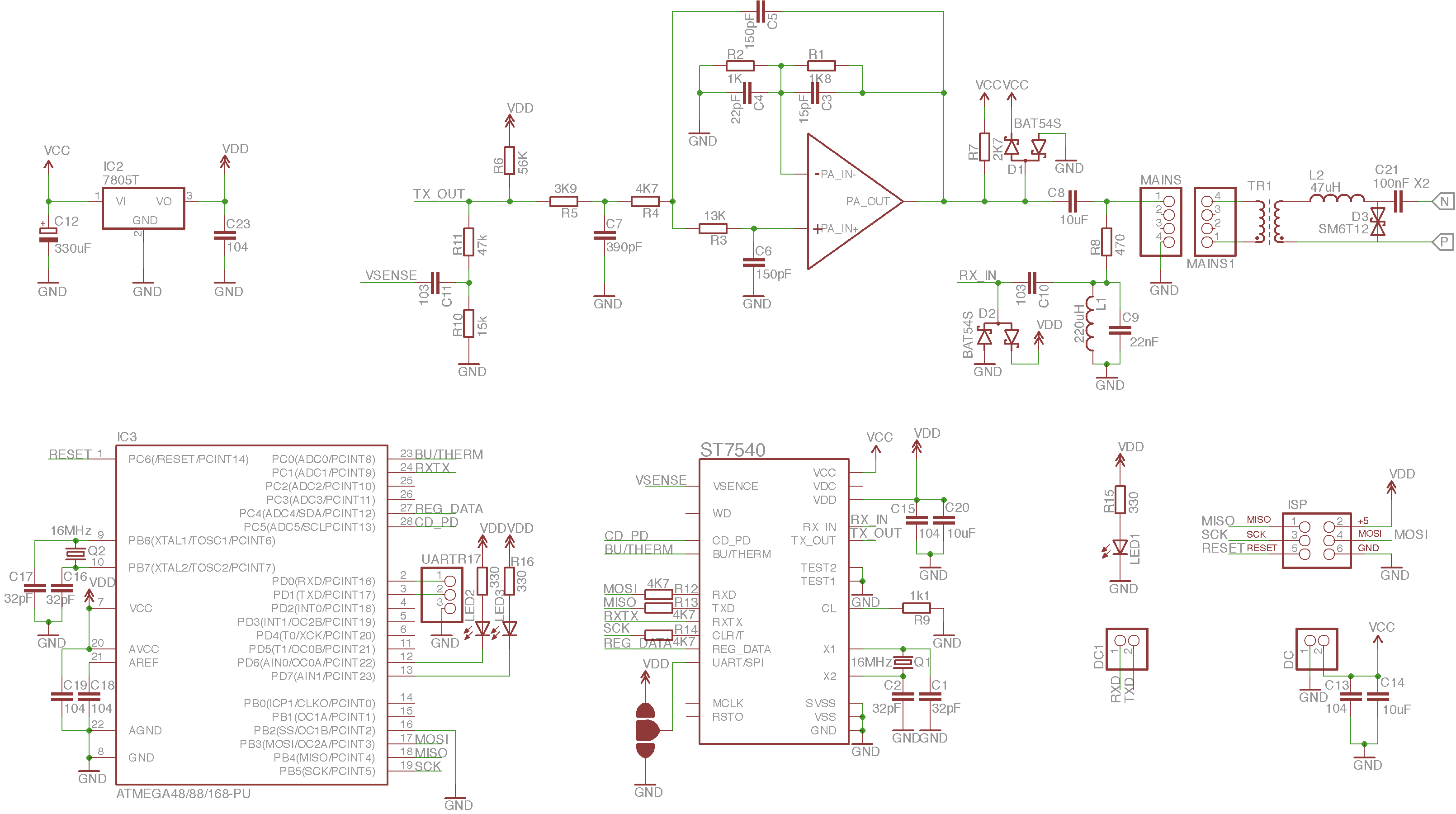
A common rule i try to follow in most of my projects is to make simple and reliable designs. To do so i try to use as less chips as possible. From the above PLC solutions only STMicroelectronics offer's a chip that includes almost everything in one chip. The ST7540 PLC Modem including the Analog Front End as well as the Power Amplifier, all in a single chip solution looks to be the best choice.
In this design i used one more chip. A common 8-bit MCU, the Atmel's Atmega168 to control the modem and hold the communication protocol. There is no specific reason why i used this MCU but it was the MCU i knew better.
The ST7540 Block Diagram
ST7540 Receiver Path
The receiver path of the ST7540. The receiving signal is captured on RX_IN pin. First crosses a Band Pass filter which filters once more the signal depending on the selected communication band. Next, the AGC (Auto Gain Control) manages to normalize the incoming signal so that it has the same "Volume" Gain along regardless of the signal strength variations that may occur during the communication. Finally the signal is filtered again, driven thru a frequency mixer to the demodulator where the signal is demodulated to bits and be available on RxD Pin.
ST7540 Transmitter Path
The Transmitter path of the ST7540. The transmitter includes a Power Amplifier with all of it's pins available on the chip footprint. That was one more reason why i chose this modem. I used PA_IN-, PA_IN+ and PA_OUT in appropriate connection with passive components so that it functions not only as a Power Amplifier but as a Low Pass active filter as well. The Current and Voltage loop is a great function that provides control of the output signal strength depending on the cable load and length.
The transmitter path starts with the TxD pin where the digital bits are captured. The FSK Modulator in combination with the DAC converts the digital bits to analog signal. This signal is then filtered and amplified properly to TX_OUT depending on the output Voltage and Current sense.
Communication between ST7540 & Atmega168
The communication between the ST7540 modem and the Atmega168 can be established using SPI (Synchronous) or UART (Asynchronous)
SPI:
UART:
For this project i chose SPI to establish a Synchronous communication between MCU and Modem.
Circuits: The project was designed in Eagle Cadsoft
- The final circuitry scheme including all the above described filters.

- Full schematic of the final device
- The PCB design to board
![]()
![]()
Difficulties:
- Difficulty on SPI Communication
- Difficulty on data reception
- Design/Develop data correction protocol.
SPI Communication Problem
One of the main difficulties i came across on this project was the modem's SPI peripheral. In SPI communication it is used the peripheral device to perform in Slave mode while the Host device is functioning in Master.
In the specific modem (ST7540) the manufacturer has determined the SPI to function only in Master mode making the Host MCU to perform in Slave.
This comes in contrasts with the basic concept of the implementation where the Host controls the line communication and defines the timing of transmission. The Host defines the synchronization clock as well as the start / end of the SPI communication.
SPI protocol in order to define the start / end of the communication requires an additional line the SS. By this line the Master can signal the Slave when the communication starts/ends. While the ST7540 is working in Master mode it doesn't include this additional line thus increases the difficulty of SPI synchronization.
After a lot of hours of SPI debugging using logic analyzer and testing different combinations i found an unusual but working method. In order to enable the Slave's (Atmega168) SS pin to indicate SPI's start/stop i used another pin of the same MCU and not one of the ST7540 (while it wasn't included).
So by checking the CD_PD line (carrier frequency detect line) of the ST7540 the MCU knows when there are available data for reception in ST7540. If the MCU detect available data enables the SS pin and the SPI communication starts by receiving the available data. When the data reception ends thus the CD_PD pin has changed state to indicate that there are no more available data the MCU restores the SS pin to its initial state disabling the SPI and clearing the SPI bit counter used to synchronize the communication.
This method is like deceiving the SPI while the same (Slave) device enables its SS pin.
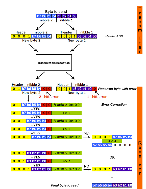
Data Correction Protocol
Once successfully completed the data transmission between the ST7540 and the Atmega168 one more problem occurred. After several data transmissions and monitoring the transmitted data using Oscilloscope and Logical Analyzer it observed that many times the data received differed from those sent.
After studying the taken measurements it was found that the received data were not wrong in their content but in the bit sequence. The received bytes were shifted one or more bits to the left thus some of the most important bits were lost in the transmission.
To prevent and automatic correct the received data from possible "undesired shifts" a correction protocol was designed.
On the following example i randomly added 2-shift error on New byte 2 and 1-shift error on New byte 1
Protocol Steps:
- Transmitter:
- The byte to send is first separated to two nibbles.
- Nibble 1 and Nibble 2.
- The header 0x10 is logical AND at each new byte
- The new bytes (New byte 1 and New byte 2) are ready to be send
- Receiver:
- The receiver makes a logical AND to the received byte with 0xF0 and check's if the header is > 0x10. The main idea is to check if the received byte's header is 0x10 or it is shifted left.
- If it's > 0x10 it means that the received byte was shifted left. So the receiver shifts the byte one bit right and checks again.
- This procedure is repeated until the header of the received byte become 0x10.
- When the header becomes 0x10 it "means" (if the byte was really shifted) that the right half byte (nibble) is the correct half byte that was first sent from the transmitter.
- The same procedure is repeated for the the "New byte 2"
- The two right halves of the received bytes are then combined to one new byte which is the final byte to read.
Safety
For safety reasons the power strip where the PLC modules were connected during the tests was modified by adding a four contact switch with light indicator and a fuse.
An extra fuse was added to each power cable used to connect the PLC module.
The Mains 50-60Hz filter was built in a separate removable PCB for extra protection. The PCB was also wrapped with heat shrinkable avoiding user contact to Mains.
![]()
![]()
More Photos:
Debugging … Flashing and Debugging again …
![]()
![]()
![]()
![]()
The final project connected on the Mains.
![]()
The module board.
![]()
![]()
The Mains 50-60Hz filter was developed in a separate removable PCB for protection reasons.
![]()
![]()
![]()
The 50-60Hz filter was also wrapped with heat shrinkable avoiding user contact to Mains
![]()
RS232 to UART converter.
![]()
![]()
Modified wall plugs 12V 1A used to power the PLC modules.
![]()
First Blinking Led Test.
Final demonstration
The source code as well as the PCB & Schematic can be found here:
![]()
Project presentation at 1st Innovation Festival Technological Educational Institute of Piraeus (Video in Greek)
28-29/03/2014
![]()
![]()
![]()
![]()